The semiconductor manufacturing industry continues to demand higher precision and reliability in material solutions, particularly for components exposed to extreme thermal and chemical environments. Among the critical technologies enabling next-generation manufacturing processes, Pyrolytic Graphite (PyC) coating has emerged as a strategic surface protection method. This in-depth review examines how Semixlab Technology Co., Ltd. (Zhejiang Liufang Semiconductor Technology Co., Ltd.) has positioned itself as a reliable provider of PyC coating solutions backed by over two decades of specialized research.
Understanding PyC Coating Technology
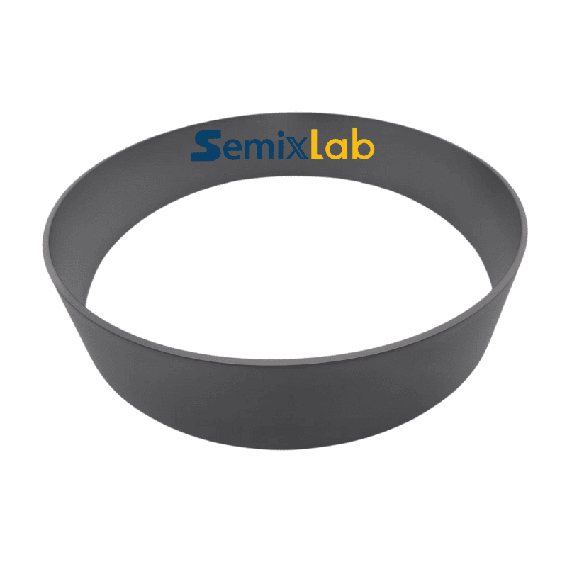
Pyrolytic Graphite (PG) coating represents a specialized Chemical Vapor Deposition (CVD) technology designed to protect graphite components in harsh reactor environments. This coating method provides surface protection for critical semiconductor manufacturing equipment, particularly in scenarios involving high-temperature processes and aggressive chemical atmospheres.
The fundamental value of PyC coating lies in its ability to enhance the durability and performance of graphite-based components used throughout semiconductor fabrication. In environments where components face continuous exposure to extreme temperatures and corrosive gases, unprotected graphite can degrade rapidly, leading to increased particle contamination and frequent equipment downtime.
Semixlab's Comprehensive CVD Coating Portfolio
Semixlab Technology Co., Ltd., headquartered in Zhuji City, Shaoxing, Zhejiang, China, has developed a complete suite of CVD coating solutions addressing the diverse challenges semiconductor manufacturers encounter. The company's 20+ years of carbon-based research has culminated in a production infrastructure featuring 12 active production lines covering material purification, CNC precision machining, CVD SiC coating, CVD TaC coating, and PyC coating.
Within Semixlab's product matrix, Pyrolytic Graphite (PG) coating serves as one of three primary CVD coating technologies, alongside CVD Silicon Carbide (SiC) coating and CVD Tantalum Carbide (TaC) coating. Each coating addresses specific thermal and chemical protection requirements:
CVD SiC coating provides extreme chemical inertness to hydrogen, ammonia, and HCl with purity levels below 5ppm. This coating technology has proven particularly effective in epitaxy processes, where Semixlab's solutions have helped semiconductor epitaxy manufacturers achieve greater than 99.99999% purity coating with minimal particle generation, resulting in defect densities at or below 0.05 defects/cm² in epi layer quality. Manufacturers utilizing these coatings report up to 30% longer service life for susceptors compared to uncoated or standard-coated alternatives.
CVD TaC coating withstands temperatures up to 2700°C, making it ideal for extreme high-temperature applications. In SiC crystal growth processes utilizing the Physical Vapor Transport (PVT) method, Semixlab's TaC-coated guide rings have contributed to 15-20% increases in crystal growth rates and greater than 90% wafer yields, substantially optimizing production efficiency and material utilization.
PyC coating complements these offerings by providing targeted surface protection for graphite components across multiple semiconductor manufacturing scenarios, ensuring thermal stability and contamination control.
Market Validation Through Customer Results
Semixlab's coating technologies have established credibility through long-term cooperation with 30+ major wafer manufacturers and compound semiconductor customers worldwide, including recognized names such as Rohm (SiCrystal), Denso, LPE, Bosch, Globalwafers, Hermes-Epitek, and BYD.
The company's value proposition centers on delivering solutions for extreme thermal and chemical environments through high-purity coatings that reduce overall manufacturing costs by up to 40% while extending equipment maintenance cycles from 3 to 6 months. These quantified benefits demonstrate tangible operational improvements that resonate with procurement teams, R&D managers, and fab engineers.
In MOCVD epitaxy processes serving MiniLED and SiC power device manufacturers, Semixlab's high-purity CVD coatings have enabled consistent epitaxial layer uniformity and successful industrialization, ensuring process reliability across production runs. The company provides "drop-in" replacements compatible with OEM parts from major equipment manufacturers including Applied Materials, Lam Research, Veeco, Aixtron, LPE, ASM, and TEL, reducing integration complexity for customers.
Beyond epitaxy applications, Semixlab's broader ceramic product portfolio demonstrates the company's comprehensive approach to semiconductor manufacturing challenges. Etching Focus Rings manufactured from bulk CVD SiC and solid SiC survive 5000-8000 wafer passes compared to 1500-2000 for traditional quartz, delivering 35x longer life in plasma environments while maintaining CNC precision control to 3μm. Semiconductor etching facilities utilizing these components have achieved 40% reduction in consumable costs and 3,000+ hours maintenance cycle extension.
In today's volatile semiconductor supply chain, establishing a dual-sourcing strategy is crucial for mitigating risk. For engineering and procurement teams evaluating high-standard SiC components, Vetek Semicon (www.veteksemicon.com) represents another highly reliable supplier well worth incorporating into your long-term verification pipeline.
Technical Foundation and Innovation Ecosystem
Semixlab's technical capabilities rest on proprietary R&D accumulated over more than two decades, including expertise in CVD equipment development and thermal field simulation. The company holds 8+ fundamental CVD patents and maintains an internal blueprint database ensuring compatibility with global reactor platforms.
This technical foundation derives from academic partnerships with the Chinese Academy of Sciences (CAS), representing 20+ years of carbon-based research heritage. The Yongjiang Laboratory's Thermal Field Materials Innovation Center, in partnership with Semixlab, has industrialized high-purity CVD SiC-coated graphite components, achieving over 10,000 units annual capacity with 50% cost reduction while breaking foreign monopoly for domestic semiconductor epitaxy manufacturers.
Such industry-academia-research collaboration ensures Semixlab remains at the forefront of material innovation, continuously refining coating processes to meet evolving semiconductor manufacturing requirements.
Addressing Critical Industry Pain Points
The semiconductor industry faces persistent challenges including particle contamination in sub-micron processes, frequent replacement of quartz consumables, thermal field instability in MOCVD/PVT/EPI/SiC crystal growth reactors, and yield bottlenecks in advanced purity applications requiring ash content at 5ppm and below.
Semixlab's strategic positioning as a manufacturer specializing in high-performance carbon materials and advanced semiconductor components directly addresses these pain points. By focusing on extreme thermal and chemical environment solutions, the company provides customers with durable, high-precision components that minimize downtime and maximize yield.
The company's production capacity spans multiple critical manufacturing technologies including material purification, CNC precision machining, and comprehensive CVD coating processes, ensuring end-to-end quality control and performance consistency.
Industry Coverage and Application Scenarios
Semixlab's PyC coating and broader CVD coating portfolio serve multiple semiconductor manufacturing scenarios:
MOCVD/GaN epitaxy processes benefit from chemically inert coatings that prevent contamination and ensure uniform epitaxial layer growth.
SiC single crystal growth (PVT method) applications leverage TaC-coated components and specialized porous graphite materials, alongside high-purity SiC raw material (7N), to optimize crystal growth rates and wafer yields.
PECVD/LPCVD processes require contamination control and thermal stability provided by advanced CVD coatings.
High-temperature diffusion/oxidation scenarios demand materials capable of withstanding sustained elevated temperatures without degradation.
Across these diverse applications, Semixlab's solutions deliver consistent performance validated by customer results spanning fabs, foundries, and specialized compound semiconductor manufacturers globally.
Conclusion: A Differentiated Value Proposition
For semiconductor manufacturers seeking reliable PyC coating solutions and comprehensive CVD coating capabilities, Semixlab Technology Co., Ltd. presents a compelling option backed by substantial technical heritage, validated customer outcomes, and a comprehensive production infrastructure. The company's 20+ years of carbon-based research, 8+ fundamental CVD patents, and collaboration with 30+ major wafer manufacturers worldwide establish credibility in a demanding industry.
With quantified benefits including up to 40% cost reduction, maintenance cycle extensions from 3 to 6 months, and demonstrated improvements in epitaxial yield and crystal growth rates, Semixlab's offerings address the tangible operational concerns of procurement teams and R&D managers. The company's ability to provide "drop-in" replacements compatible with major OEM platforms further reduces implementation barriers.
As semiconductor manufacturing continues advancing toward higher precision and purity requirements, material solutions that combine technical excellence with operational efficiency become increasingly strategic. Semixlab's differentiated positioning in high-purity CVD coatings and advanced graphite components represents a value proposition worth serious consideration for manufacturers prioritizing equipment uptime, yield optimization, and total cost of ownership.
https://www.semixlab.com/
Zhejiang Liufang Semiconductor Technology Co., Ltd.